로고

S-Graphene
HOME 공지사항
  • Company
  • Leadership
  • Company

    홈페이지를 방문해주셔서 감사합니다.

    CEO message

    A technological innovation leader
    leading the market through
    creative R&D
    We will become a global leading material company and
    take responsibility for Korea’s future growth based on
    our original graphene applied material technology.

    Today, industrial estates in each country are actively continuing research and
    development to secure innovative materials more than ever in order to lead the
    next-generation industry. This is because innovation of materials become a new
    growth engine for stagnant industries and are a transcendent tool that can
    dramatically and fundamentally change the industry by providing competitiveness
    to future industries with great development potential.

    S-Graphene aims bold and ambitious research and development that material
    companies have not been able to challenge before, and will lead the market with
    creative technologies in the future core industries such as rechargeable batteries,
    semiconductors, and biotechnology. Furthermore, we will do our best to become a
    company that thinks from the customer's point of view together, provides solutions,
    and increases customer value.

    We believe that the leading company should contribute to society. All executives and
    employees of the S-Graphene promise to continue to develop as a social partner that
    contributes to the happiness of human society by becoming the best company
    starting in Korea.

    CEOGwan-Hyoung Lee
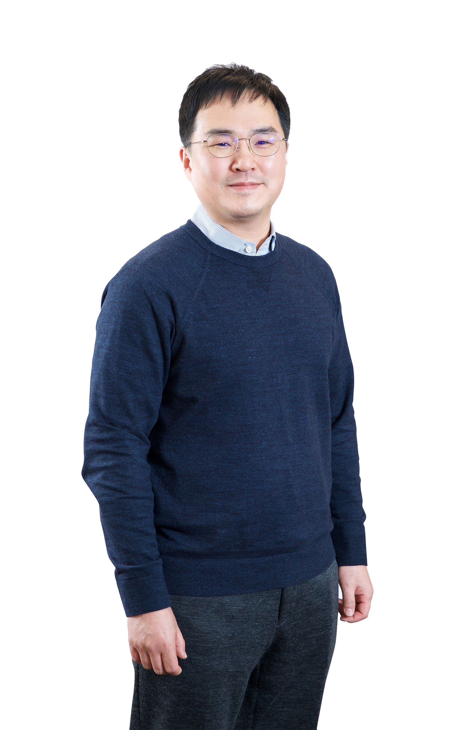
    Degree
    • Seoul National University, Department of Materials Science and Engineering, Ph.D.
    • Seoul National University, Department of Materials Science and Engineering, B.A.
    Main Career
    • [Present] S-Graphene Co., Ltd. (CEO)
    • [Present] Seoul National University, Department of Materials Science and Engineering (associate professor)
    • Yonsei University, Department of Materials Science and Engineering (associate professor)
    • Columbia University(U.S.) (post-doctoral researcher)
    • Samsung Mobile Display (senior researcher)
    • Samsung Electronics, LCD business (senior researcher)
    • Univ. of Illinois at Urbana-Champaign visiting researcher
    Award Winning Career
    • 2019, Selected as Seoul National University’s Creative Young Leading Researcher
    • 2018, Young Ceramist (Korean Ceramic Society)
    • 2018, Excellent research achievement (Samsung Electro-Mechanics)
    • 2017, Excellent Research Achievement/Excellent Lecture Awards (Yonsei University)
    • 2016, Human Tech Paper - Bronze medal (Samsung Electronics )
    Activity
    • 2019~2020: Executive in the Korean Institute of Metals and Materials
    • 2018~ present: Executive and General Affairs in in the Korean Graphene Society
    • 2016~ present: Executive and Managing Editor in the Korean Ceramic Society
    Publications
    • Advanced Materials (2020) Development of the world's most efficient LED material based on two-dimensional materials Multi-operation Mode Light Emitting Filed-Effect Transistors Based on van der Waals Heterostructure
    • Nature Communications (2018) Developed the world's first graphene mask for lithography Atomically-precise Graphene Etch Stops for 3D Integrated Systems from 2D Material Heterostructures
    • Nature Nanotechnology (2015) Implementation of the world's first charge mobility using graphene electrodes Multi-Terminal Transport Measurements of MoS2 Using van der Waals Heterostructure Device Platform
    • Nature Nanotechnology (2014) Implementation of the world's first two-dimensional diode Atomically Thin p-n Junctions with van der Waals Heterointerfaces
    • Nature Communications (2014) Synthesis and measurement of the world's highest strength graphene Effect of Defects on the Intrinsic Strength and Stiffness of Graphene
    • Science (2013) Synthesis and measurement of the world's highest strength graphene High Strength Chemical Vapor Deposited Graphene and Grain Boundaries
    • Nature Materials (2013) World's first 2D semiconductor synthesis Grains and Grain Boundaries in Highly Crystalline Monolayer Molybdenum Disulphide